WSe2 (Tungsten Diselenide)
 WSe2 is a semiconductor with an indirect band gap of ~1.3 eV, monolayer WSe2 has a direct band gap. The layers are stacked together via van der Waals interactions and can be exfoliated into thin 2D layers. Tungsten Diselenide belongs to the group-VI transition metal dichalcogenides (TMDC).
To buy WSe2 crystals please click here.
WSe2 is a semiconductor with an indirect band gap of ~1.3 eV, monolayer WSe2 has a direct band gap. The layers are stacked together via van der Waals interactions and can be exfoliated into thin 2D layers. Tungsten Diselenide belongs to the group-VI transition metal dichalcogenides (TMDC).
To buy WSe2 crystals please click here.
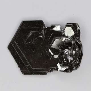
The WSe2 crystals produced at HQ Graphene have a typical lateral size of ~0.8-1 cm, are hexagonal shaped and have a metallic appearance.
We produce both n-type and p-type WSe2, having typical charge carrier densities of ~1015cm-3 at room temperature.
A selection of peer review publications on the WSe2 we sell can be found below.
| Crystal size | ~10 mm |
| Electrical properties | Semiconductor, p-type (we also have n-type available) |
| Crystal structure | hexagonal |
| Unit cell parameters | a = b = 0.328 nm, c = 1.298 nm, α = β = 90°, γ = 120° |
| Monolayer properties | |
| Type | Synthetic |
| Purity | >99.995 % |
| Characterized by | XRD, Raman, EDX, Hall measurement |
| More information? | Please contact us by email or phone |
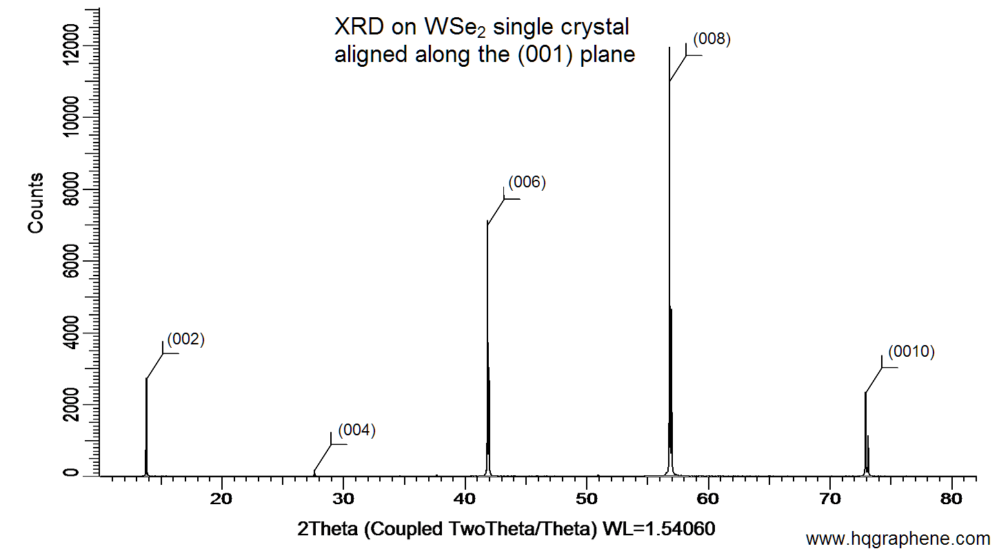
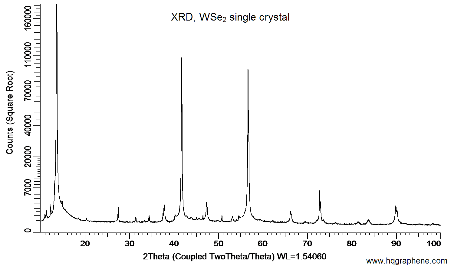
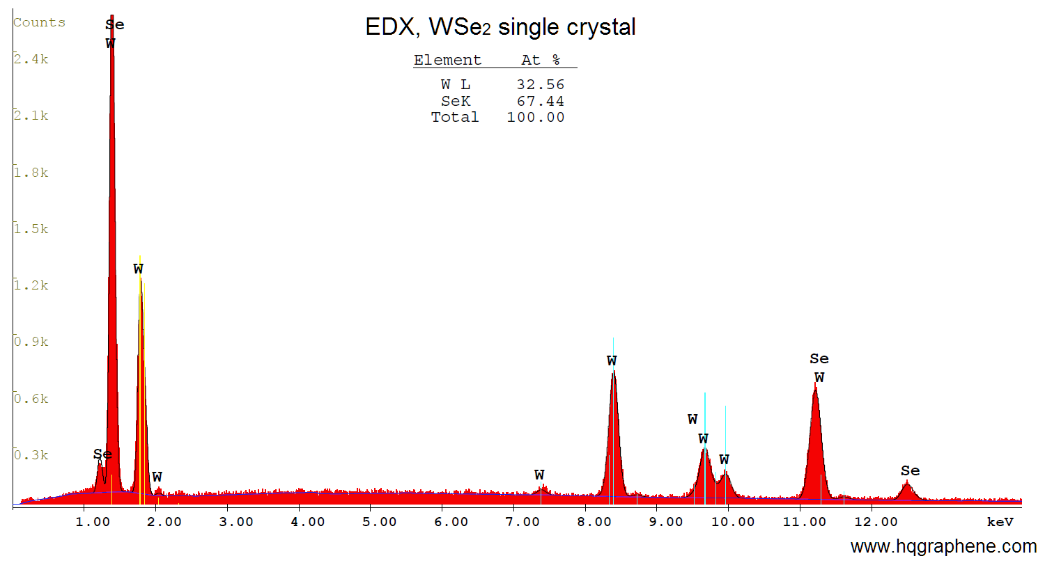
The single crystal WSe2 is characterized using:
XRD: single crystal and powder X-ray diffraction (D8 Venture Bruker and D8 Advance Bruker)EDX: Energy-dispersive X-ray spectroscopy for stoichiometric analysis
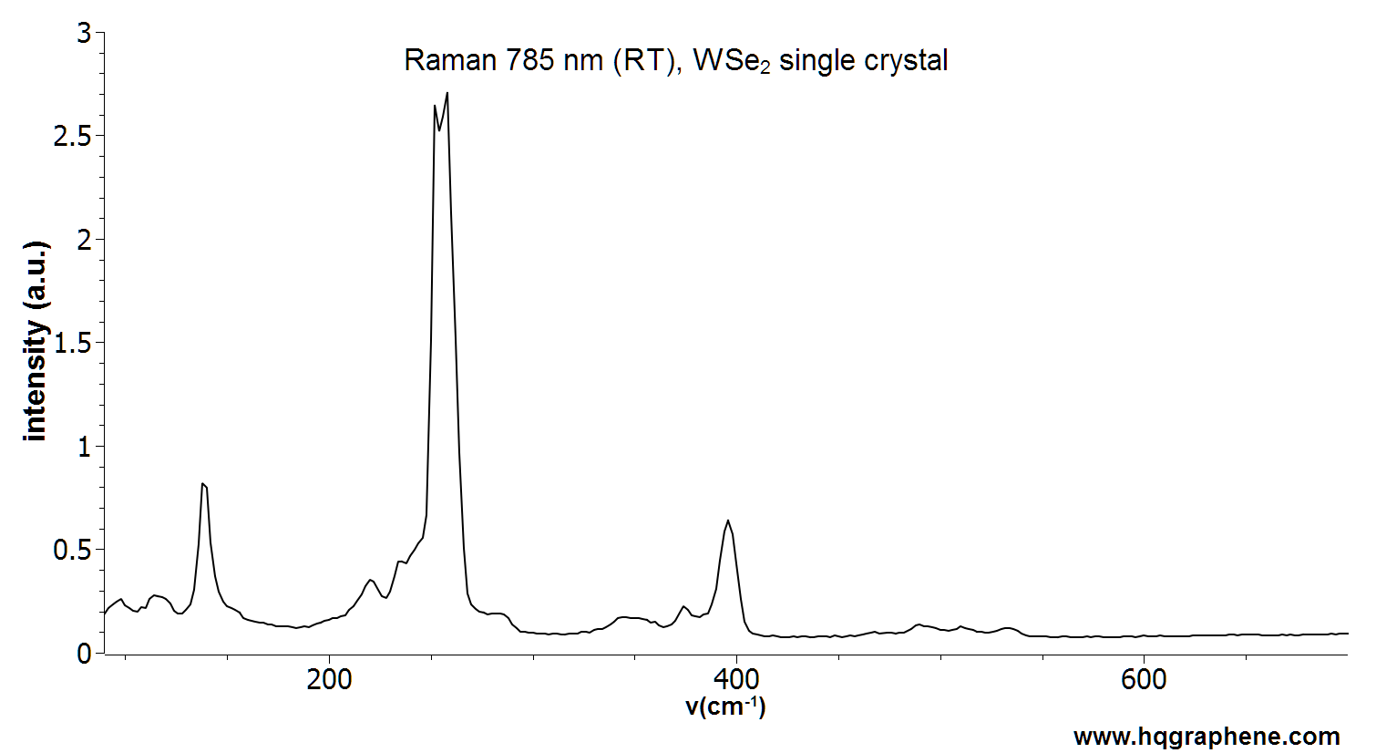
Raman: 785 nm Raman system
Hall measurement: Extraction of charge carrier density and doping in the Van der Pauw geometry.
Raman, XRD and EDX on WSe2:
Click on an image to zoom
HQ Graphene Wiki on:
WSe2 (Tungsten Diselenide)
1. Shin, Y.S., et al. "Li Intercalation Effects on Interface Resistances of High‐Speed and Low‐Power WSe2 Field‐Effect Transistors." Advanced Functional Materials 30.45 (2020): 2003688.
2. Wang, Z., et al. "Broadband photodetector based on ReS2/graphene/WSe2 heterostructure." Nanotechnology 32.46 (2021): 465201.
3. Fülöp, B., et al. "Boosting proximity spin-orbit coupling in graphene/WSe2 heterostructures via hydrostatic pressure." npj 2D Materials and Applications 5.1 (2021): 82.
4. Cho, C., et al. "Highly strain-tunable interlayer excitons in MoS2/WSe2 heterobilayers." Nano letters 21.9 (2021): 3956-3964.