GaSe (2H phase Gallium Selenide)
 GaSe (2H phase) is a semiconductor with an indirect band gap of ~2.1 eV. GaSe has been used as a semiconductor, photoconductor, a second harmonic generation crystal in nonlinear optics and as a far-infrared conversion material.
The layers are stacked together via van der Waals interactions and can be exfoliated into thin 2D layers. GaSe belongs to the group-13 post-transition metal monochalcogenides.
To buy GaSe crystals please click here.
GaSe (2H phase) is a semiconductor with an indirect band gap of ~2.1 eV. GaSe has been used as a semiconductor, photoconductor, a second harmonic generation crystal in nonlinear optics and as a far-infrared conversion material.
The layers are stacked together via van der Waals interactions and can be exfoliated into thin 2D layers. GaSe belongs to the group-13 post-transition metal monochalcogenides.
To buy GaSe crystals please click here.
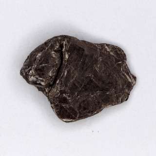
The 2H phase of Gallium Selenide has a typical lateral size of ~0.6-0.8 cm and has a dark-copper metallic appearance.
| Crystal size | ~8 mm |
| Electrical properties | Semiconductor |
| Crystal structure | Hexagonal |
| Unit cell parameters | a = b = 0.374 nm, c = 1.592 nm, α = β = 90°, γ =120° |
| Monolayer properties | |
| Type | Synthetic |
| Purity | >99.995 % |
| Characterized by | XRD, Raman, EDX |
| More information? | Please contact us by email or phone |
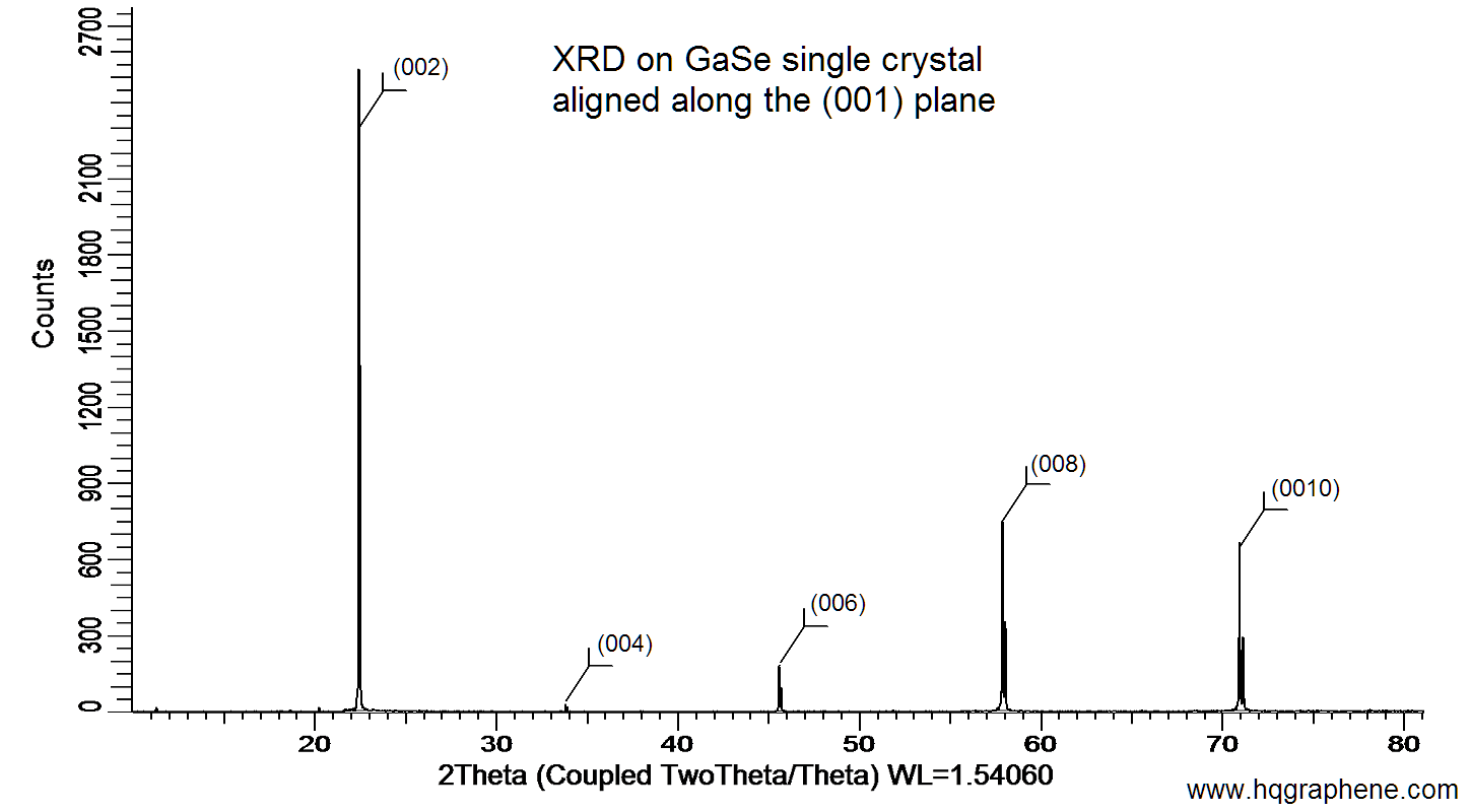
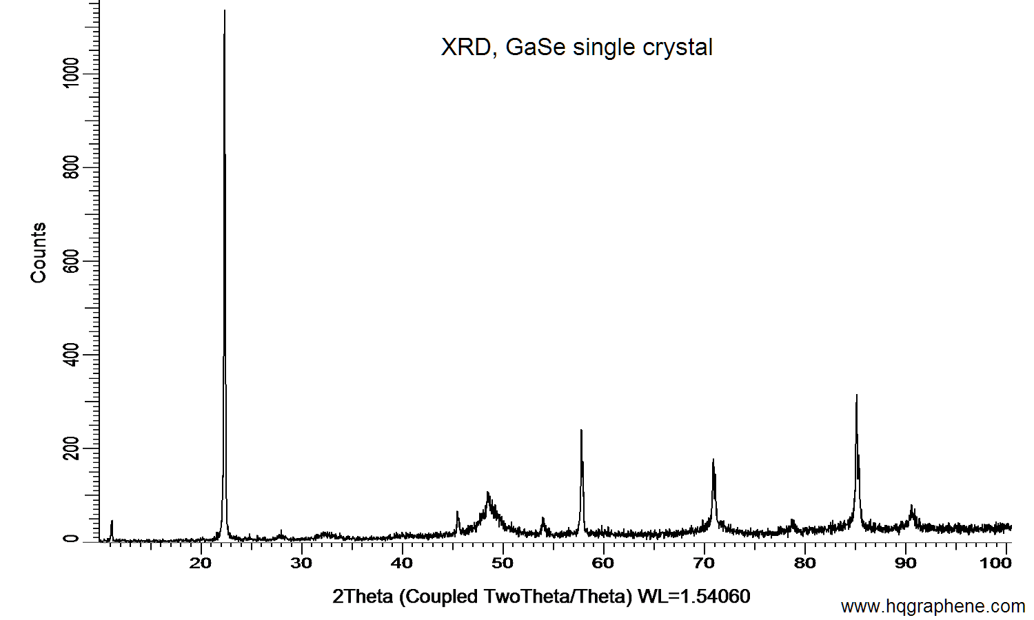
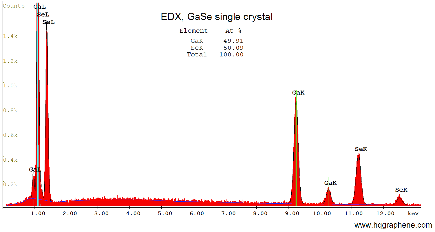
The single crystal GaSe is characterized using:
XRD: single crystal and powder X-ray diffraction (D8 Venture Bruker and D8 Advance Bruker)EDX:Energy-dispersive X-ray spectroscopy for stoichiometric analysis
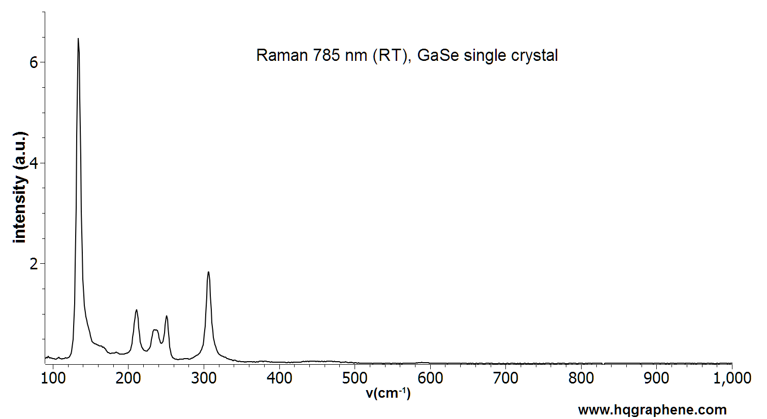
Raman: 785 nm Raman system
Raman, XRD and EDX on GaSe:
Click on an image to zoom
HQ Graphene Wiki on:
GaSe (Gallium selenide)
1. Maeso, David, et al. "Strong modulation of optical properties in rippled 2D GaSe via strain engineering." Nanotechnology 30.24 (2019): 24LT01.
2. Ryousuke, Ishikawa, et al. "Photovoltaic Characteristics of GaSe/MoSe 2 Heterojunction Devices." Nanoscale Research Letters 16.1 (2021).
3. Guo, Feng, et al. "Multifunctional optoelectronic synapse based on ferroelectric van der Waals heterostructure for emulating the entire human visual system." Advanced Functional Materials 32.6 (2022): 2108014.