GeP (Germanium Phosphide)
 GeP is a semiconductor 2D material having a bandgap of ~1.68eV for monolayers and ~0.51eV for bulk crystals. The layers are stacked together via van der Waals interactions and can be exfoliated into thin 2D layers.
To buy GeP crystals please click here.
GeP is a semiconductor 2D material having a bandgap of ~1.68eV for monolayers and ~0.51eV for bulk crystals. The layers are stacked together via van der Waals interactions and can be exfoliated into thin 2D layers.
To buy GeP crystals please click here.
The GeP crystals produced at HQ Graphene have a typical lateral size of ~0.1-0.3 cm, hexagonal shaped and have a metallic appearance.
More information about the GeP crystals we sell can be found below.
GeP crystal properties
| Crystal size | ~3 mm |
| Electrical properties | Semiconductor |
| Crystal structure | Monoclinic |
| Unit cell parameters | a = 1.519 nm, b = 0.368 nm, c = 0.918 nm, α = γ = 90°, β = 101.560° |
| Type | Synthetic |
| Purity | >99.995 % |
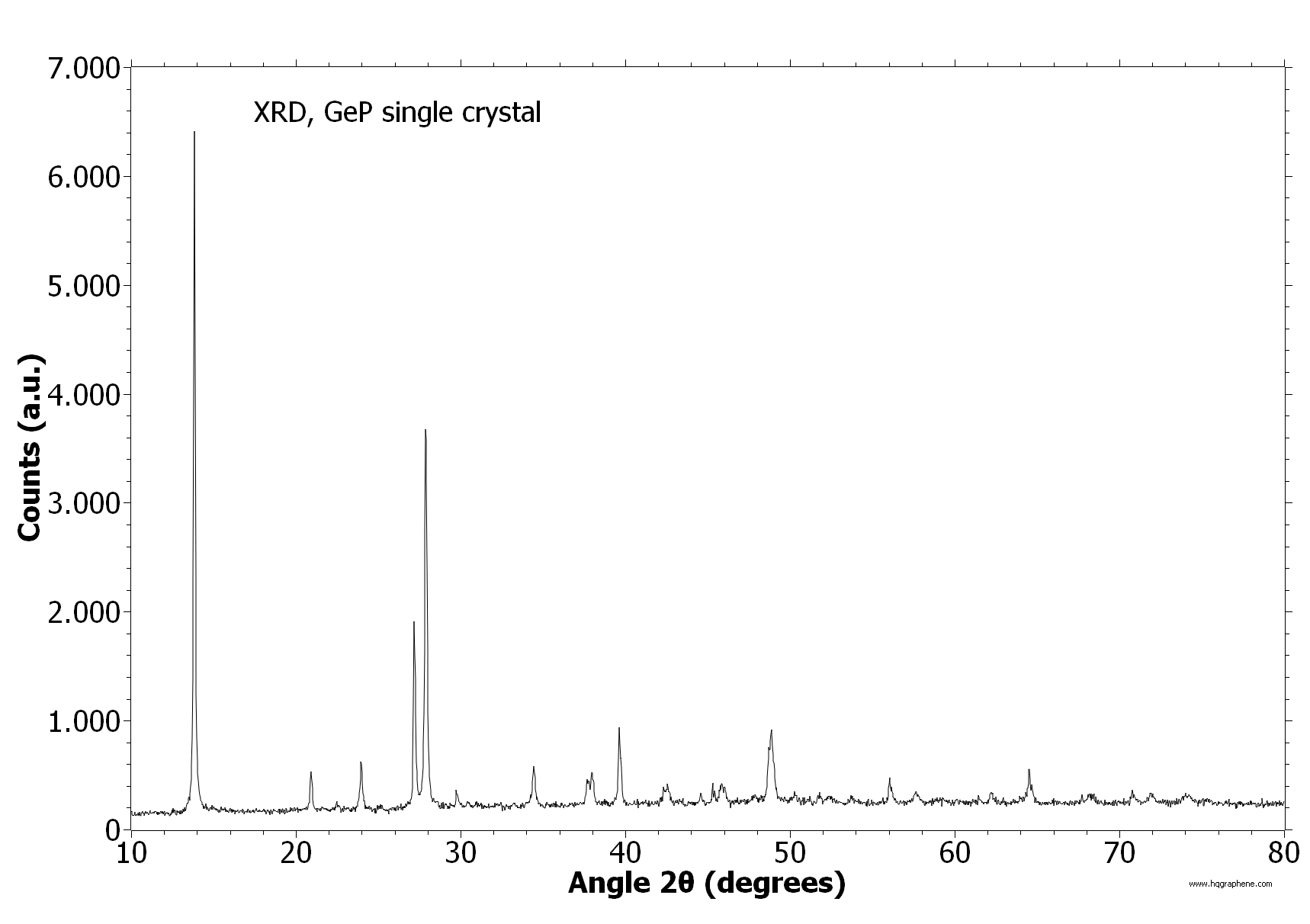
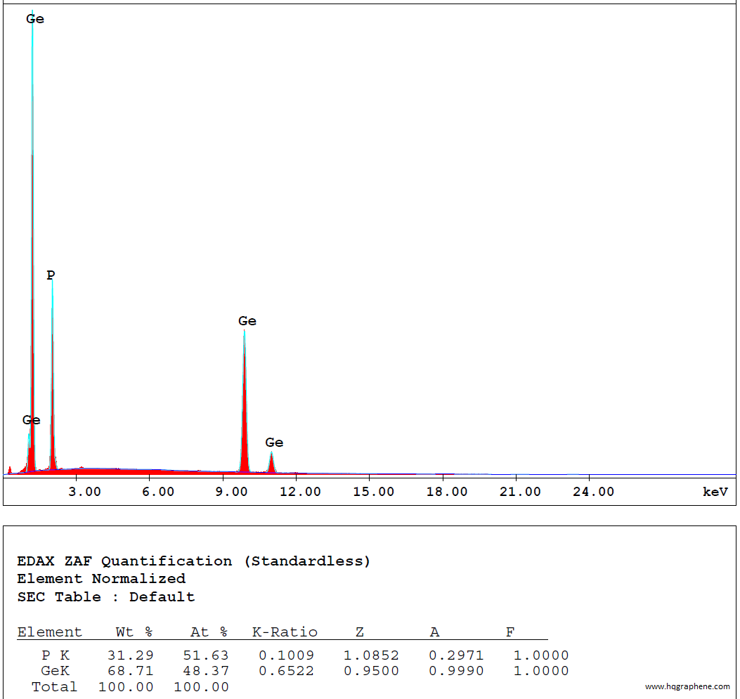
| Characterized by | XRD, EDX |
| More information? | Please contact us by email or phone |
The single crystal GeP is characterized using:
XRD: single crystal and powder X-ray diffraction (D8 Venture Bruker and D8 Advance Bruker)EDX: Energy-dispersive X-ray spectroscopy for stoichiometric analysis
XRD and EDX on GeP:
Click on an image to zoom